
Diamond: The Future of Semiconductor Cooling
As AI processors become more powerful, thermal management is emerging as one of the biggest challenges in semiconductor engineering. This post explores how Chemical Vapor Deposition (CVD) diamond is being developed as an advanced thermal management material, enabling faster heat dissipation, improved chip performance, and the next generation of AI, 3D integrated circuits, and high-power semiconductor devices..
8/5/20261 min read
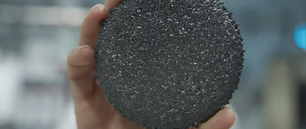
As semiconductor devices continue to scale, performance is no longer limited solely by transistor density—it is increasingly constrained by thermal management.
The industry has spent decades optimizing transistor architectures through FinFETs, GAAFETs, advanced packaging, and 3D heterogeneous integration. However, these innovations have also pushed power density and localized heat flux to unprecedented levels. In advanced AI accelerators and RF devices, self-heating has become one of the primary barriers to achieving higher clock frequencies, greater power density, and long-term device reliability.
This is where Chemical Vapor Deposition (CVD) Diamond is emerging as a transformative material.
Unlike conventional heat spreaders that dissipate heat after it has already reached the package, CVD diamond enables junction-level thermal management by integrating an ultra-high thermal conductivity layer directly onto semiconductor devices.
Why diamond?
• Thermal conductivity exceeding 2,000 W/m·K, nearly 5× higher than copper.
• Exceptional phonon transport characteristics for rapid heat extraction.
• Electrical insulation combined with outstanding thermal conductivity.
• Chemical stability and radiation hardness, making it ideal for aerospace and defense electronics.
Recent breakthroughs have demonstrated low-temperature (300–400°C) CVD diamond growth, making post-fabrication integration compatible with modern semiconductor manufacturing. This addresses one of the biggest historical challenges of diamond integration.
Research groups are now demonstrating:
✅ Diamond thermal matrices for 3D Integrated Circuits (3D-ICs)
✅ GaN-on-Diamond HEMTs with significantly reduced junction temperatures
✅ Record-low thermal boundary resistance (TBR) at Diamond/GaN interfaces
✅ Device-level cooling for high-power RF amplifiers operating at extreme power densities
The implications extend far beyond cooling.
Lower junction temperatures directly improve:
• Carrier mobility
• Device reliability (MTTF)
• Electromigration resistance
• Power efficiency
• Leakage current reduction
• Operating frequency
• Thermal design power (TDP) headroom
As AI computing continues to demand increasingly dense GPU and accelerator architectures, thermal engineering is becoming as critical as transistor engineering itself.
The next frontier in semiconductor innovation may not be another transistor architecture—but the materials surrounding it.
CVD diamond is rapidly evolving from a specialty material into a strategic enabler for next-generation semiconductor devices, AI infrastructure, wide-bandgap power electronics, RF communication systems, and advanced packaging.
The future of semiconductor scaling will depend not only on smaller transistors, but also on better thermal pathways.
Hours
Monday - Friday
9:00 am - 6:00 pm
Location
+91 9343002868
samratinnovationsinc@gmail.com sales@samratinnovations.com
Contact
No. 878 ,BEML Layout Road Dwaraka Nagar ,Channasandra Rajarajeshwari Nagar Bangalore-98 ,India