
The Economics of India’s Semiconductor Ambitions: What Does a ₹91,526 Crore Fab Actually Buy?
An analytical look at the economics behind Tata Electronics’ ₹91,526 crore Dholera semiconductor fab, from wafer capacity and chip output to revenue and gross-profit scenarios. Using industry benchmarks and illustrative assumptions, the post explores what it could take to turn large-scale semiconductor manufacturing capacity into sustainable economic value.
8/19/20266 min read
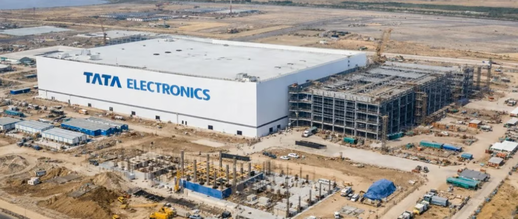
The Economics of India’s Semiconductor Ambitions: What Does a ₹91,526 Crore Fab Actually Buy?
India's semiconductor ambitions are moving from policy announcements to physical manufacturing infrastructure.
At the centre of this transition is Tata Electronics' planned semiconductor fabrication facility in Dholera, Gujarat, being developed in partnership with Taiwan's Powerchip Semiconductor Manufacturing Corporation (PSMC).
With a planned investment of ₹91,526 crore, the project represents one of the largest investments in India's semiconductor manufacturing ecosystem.
But what does that investment actually buy?
And more importantly, what would it take for a fab of this scale to generate an attractive economic return?
The Scale of the Dholera Fab
The headline numbers are significant:
₹91,526 crore — approved project investment
50,000 wafers/month — planned capacity
300 mm (12-inch) — wafer size
28–110 nm — planned process technologies
At the stated capacity, the fab would have an annualised wafer-start capacity of:
50,000 × 12 = 600,000 wafers/year
That is a substantial manufacturing footprint.
However, there is an important distinction that is easy to overlook:
A wafer is not a chip.
A semiconductor fab does not sell "wafers" simply as units of silicon area. The economic value ultimately comes from the integrated circuits that can be manufactured on those wafers, the yield achieved, and the value of those products in the market.
How Many Chips Can One Wafer Produce?
A 300 mm wafer has approximately 70,700 mm² of silicon area.
The number of chips that can be produced from each wafer depends on several factors, including:
Die size
Wafer utilisation
Manufacturing yield
Product design
Process technology
Product mix
For example, consider a hypothetical 50 mm² die.
Ignoring edge losses, approximately:
70,700 ÷ 50 ≈ 1,414 dies
could theoretically fit within the wafer's silicon area.
If we then assume a hypothetical 90% manufacturing yield, this could translate to approximately:
1,414 × 90% ≈ 1,273 usable dies per wafer
This is only an illustrative calculation. Actual die-per-wafer calculations also need to account for the geometry of the wafer, die placement, edge exclusion, test structures and other manufacturing considerations.
At 600,000 wafers per year, even a relatively large die could therefore result in hundreds of millions of usable chips annually.
For smaller products, the number could move significantly higher.
This is particularly relevant because the Dholera fab is planned to target analog and logic products across the 28–110 nm range, including applications such as power management, display drivers and microcontrollers.
But this is where semiconductor economics becomes much more interesting.
More Chips Does Not Automatically Mean More Profit
It is tempting to look at a number such as 600,000 wafers per year and conclude that the fab could produce an enormous number of semiconductor devices.
That is true.
But volume alone does not determine whether a semiconductor fab is economically successful.
A fab is an extraordinarily capital-intensive asset.
The economics depend on questions such as:
How much revenue can each wafer generate?
How quickly can the fab reach high utilisation?
What manufacturing yield can it achieve?
What products are being manufactured?
What prices can those products command?
How much does each wafer cost to process?
How much capacity is secured by customers?
How much additional capital expenditure is required over time?
To explore this, we can use established semiconductor foundries as reference points.
What Do Established Foundries Generate?
In 2025, GlobalFoundries reported:
US$6.79 billion revenue
Approximately 2.3 million 300 mm-equivalent wafer shipments
24.9% gross margin
Meanwhile, United Microelectronics Corporation (UMC) reported:
NT$237.6 billion revenue
29.0% gross margin
More than 400,000 12-inch-equivalent wafers/month of capacity
These companies operate across multiple process technologies, geographies and product categories.
Therefore, their financial metrics cannot simply be transferred to Tata Electronics' Dholera fab.
However, they provide useful industry benchmarks for understanding the economics of large-scale foundry operations.
A Simple Economic Scenario for Dholera
Let's now consider a simplified scenario.
The Dholera fab has a stated full-capacity level of:
600,000 wafers/year
But a fab does not necessarily operate at 100% utilisation from day one.
So let's assume an illustrative 85% utilisation.
That gives:
600,000 × 85% = 510,000 wafers/year
Now we need to estimate how much revenue those wafers could generate.
Instead of assuming a selling price for individual chips, we can use a simplified wafer-level revenue assumption.
Suppose the fab generated an illustrative:
US$5,000 revenue per wafer
Then annual revenue would be:
510,000 × $5,000
= US$2.55 billion
Again, this is an illustrative scenario, not a forecast of Tata Electronics' actual wafer pricing.
Wafer revenue can vary substantially depending on process technology, product mix, die size, customer contracts, yields and market conditions.
What If the Fab Achieved a 27% Gross Margin?
For another illustrative assumption, consider a 27% gross margin.
This sits between the FY2025 gross margins reported by GlobalFoundries and UMC:
GlobalFoundries: 24.9%
UMC: 29.0%
Applying a 27% gross margin to the hypothetical US$2.55 billion revenue:
$2.55B × 27%
≈ US$689 million gross profit per year
Now compare that figure with the headline project investment of:
₹91,526 crore
At an exchange rate of roughly ₹87 per US dollar, that investment is approximately US$10.5 billion.
A simple comparison gives:
$10.5B ÷ $689M ≈ 15 years
So, under this simplified scenario, the annual gross profit would represent roughly 15 years of gross-profit-equivalent contribution relative to the headline project investment.
But there is a very important caveat.
This Is Not a 15-Year Payback Period
The calculation above should not be interpreted as Tata Electronics' actual payback period.
Gross profit is not the same as free cash flow.
A real semiconductor investment model would need to consider:
Operating expenses
R&D
Selling and administrative costs
Depreciation
Financing costs
Taxes
Working capital
Maintenance and expansion capex
Ramp-up costs
Yield learning
Customer acquisition
Capacity utilisation over time
The fab is also unlikely to operate at 85% utilisation immediately after commercial production begins.
A realistic financial model would therefore require a multi-year ramp-up and cash-flow analysis rather than simply dividing project investment by annual gross profit.
The 15-year figure is therefore best understood as a simple gross-profit-to-investment comparison, not a predicted return period.
The Role of Government Support
There is another important factor in understanding the economics of the project.
The Government of India has provided fiscal support for eligible project costs under the semiconductor incentive framework.
This changes the effective capital burden of the project.
However, the 50% support should not simply be interpreted as "the government pays 50% of the ₹91,526 crore headline investment."
The applicable support is based on eligible project costs and the relevant scheme conditions.
Therefore, any detailed investment-return model would need to incorporate the actual eligible-cost structure and government disbursement schedule.
What Really Determines Fab Economics?
The exercise highlights an important point about semiconductor manufacturing.
A fab isn't economically successful simply because it can manufacture a large number of chips.
The real challenge is converting enormous amounts of invested capital into high-value, consistently manufactured products.
That requires several things to work simultaneously:
1. High utilisation
A billion-dollar-plus manufacturing facility generates value only when its expensive equipment is being used productively.
Unused fab capacity represents a significant opportunity cost.
2. High yield
A wafer can contain thousands of potential dies, but the economics depend on how many of those dies ultimately become sellable products.
Higher yields mean more good chips from the same manufacturing input.
3. The right product mix
Not every chip generates the same economic value.
A fab producing different analog, logic, power-management or microcontroller products can have very different revenue-per-wafer economics depending on product complexity, die size and market pricing.
4. Secured customers
A fab needs customers capable of filling its capacity over many years.
Long-term customer relationships and predictable demand are therefore as important as manufacturing capability.
5. Process competitiveness
The 28–110 nm range is not the leading edge of semiconductor manufacturing, but these mature and specialty process technologies remain important across automotive, industrial, consumer, power and other applications.
The opportunity is therefore not simply about manufacturing the smallest possible transistor.
It is about manufacturing the right products at the right cost, yield and scale.
The Bigger Picture
The Dholera fab represents something larger than a single manufacturing project.
It is an attempt to build semiconductor manufacturing capability in India at a scale that can support domestic demand while integrating the country more deeply into the global semiconductor supply chain.
The headline number — ₹91,526 crore — tells us the scale of the investment.
The 50,000 wafers/month figure tells us the scale of the manufacturing capacity.
But the real economic question is what happens between those two numbers.
How much revenue can each wafer generate?
How quickly can utilisation ramp up?
What yields can be achieved?
Which customers will fill the capacity?
And ultimately, how much economic value can be generated from every wafer processed?
That is the real economics behind semiconductor manufacturing.
A semiconductor fab isn't economically won by manufacturing the maximum number of chips. It is won by keeping expensive capacity utilised, achieving high yields, securing customers and generating sufficient value from every wafer processed.
India's semiconductor story is therefore not just about building fabs.
It is about building a manufacturing ecosystem capable of turning massive capital investment into sustainable technological and economic value.
Methodology Note
The calculations in this article combine publicly reported industry data with illustrative assumptions.
The following are assumptions used solely to demonstrate semiconductor economics:
85% utilisation
US$5,000 revenue per wafer
27% gross margin
90% yield in the illustrative die-count example
These assumptions are not forecasts of Tata Electronics' actual production, pricing, margins, profitability or payback period.
The ~15-year figure is a gross-profit-to-investment comparison, not a formal investment payback calculation.
#Semiconductors #SemiconductorEconomics #SemiconductorManufacturing #India #ChipManufacturing #TataElectronics #Dholera #Manufacturing #SamratInnovations
Hours
Monday - Friday
9:00 am - 6:00 pm
Location
+91 9343002868
samratinnovationsinc@gmail.com sales@samratinnovations.com
Contact
No. 878 ,BEML Layout Road Dwaraka Nagar ,Channasandra Rajarajeshwari Nagar Bangalore-98 ,India